

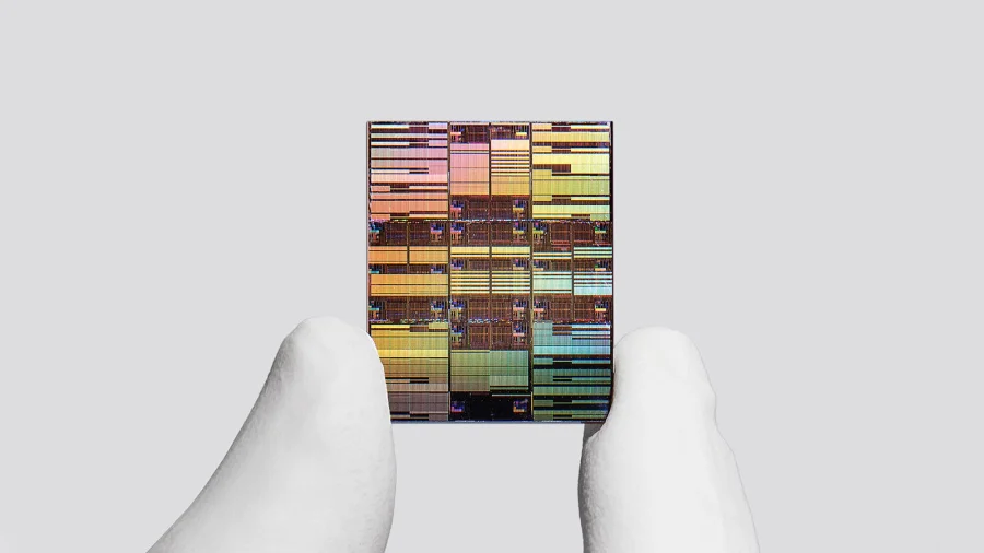

IBM has announced a major breakthrough in semiconductor technology, claiming to have created the world’s first sub-1 nanometer chip. The new chip technology, which measures just 0.7 nanometers, is powered by a new design called nanostack architecture. This development is expected to lead to more powerful and efficient chips in the coming years.
What is the 0.7nm Chip Technology?
The new chip technology is the world’s first to go below the 1 nanometer mark. According to IBM Research, it is a 0.7nm chip technology that uses a new nanostack architecture. This structure is designed to improve performance and energy efficiency, making it a significant step forward for the semiconductor industry.
IBM described the design as a ‘block of flats’ breakthrough, as reported by BBC News. This analogy refers to the way the transistors are stacked vertically, similar to floors in a building, allowing for more components in a smaller space.
Why This Matters for the Future of Chips
This breakthrough is important because smaller chips generally mean faster and more energy-efficient devices. The sub-1 nanometer technology could eventually be used in everything from smartphones to supercomputers, enabling new capabilities that are not possible with current chip designs.
IBM’s announcement, covered by Reddit’s technology community, highlights the company’s continued leadership in semiconductor research. The new nanostack architecture is a key part of this innovation, as it allows for more transistors to be packed into a tiny area without sacrificing performance.
Our Take: A Promising Step, But Commercial Reality is Years Away
In our view, IBM’s sub-1 nanometer chip is an impressive engineering achievement. However, readers should understand that this is a research breakthrough, not a product ready for the market. It will likely take several years before this technology appears in consumer devices. The real test will be whether IBM can move this from the lab to mass production, which is a challenge that has tripped up many previous chip innovations. Still, this is a clear signal that the race to make chips smaller and more powerful is far from over.