

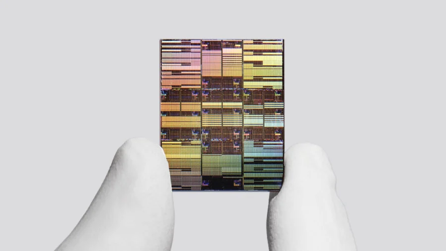

IBM has announced a major breakthrough in semiconductor technology, claiming the world’s first sub-1 nanometer chip. The new chip architecture, built at the 0.7 nm (7 angstrom) node, can pack nearly 100 billion transistors onto a chip the size of a human fingernail. That is nearly double the transistor density of IBM’s previous generation of chip technology.
According to IBM's official announcement, the breakthrough is designed specifically for AI data centers. The company says the new technology will deliver a significant improvement in both compute performance and energy efficiency.
What the sub-1 nanometer chip means for computing
Jay Gambetta, director of IBM Research and IBM Fellow, described the achievement in an advance media briefing. "It's not just an incremental step, it's a meaningful leap forward," he said. Gambetta added that the new chip technology is "pointing to a future where computing becomes significantly more powerful without a corresponding increase in energy."
The sub-1 nanometer node is a major milestone in the chip industry. For years, manufacturers have been pushing to shrink transistors to fit more on a single chip. Smaller transistors generally mean faster processing and lower power consumption. IBM’s new 0.7 nm node takes that trend to a new level.
IBM’s new chip technology for AI data centers
The announcement comes five years after IBM unveiled its 2 nm node chips, as noted by Fast Company. The new sub-1 nm architecture could unlock massive power savings for AI applications, which are increasingly demanding more computing power.
According to Ars Technica, the technology represents a "meaningful leap forward" in chip design. The nearly 100 billion transistors on a fingernail-sized chip mean that AI models can run faster and more efficiently, without requiring more energy.
Our Take: A genuine leap, but challenges remain
IBM’s claim of the world’s first sub-1 nanometer chip technology is genuinely impressive. Doubling transistor density on a chip that small is an engineering feat. The promise of more powerful computing without a corresponding increase in energy is exactly what the AI industry needs right now.
However, it is important to remember that this is a technology announcement, not a product launch. Moving from a lab breakthrough to mass production is a long and difficult road. IBM will need to work with manufacturing partners to bring this to market. Still, this is a clear signal that the race to smaller, more efficient chips is far from over. For businesses and consumers, it means that the next generation of AI hardware could be significantly more capable — and that is good news.
